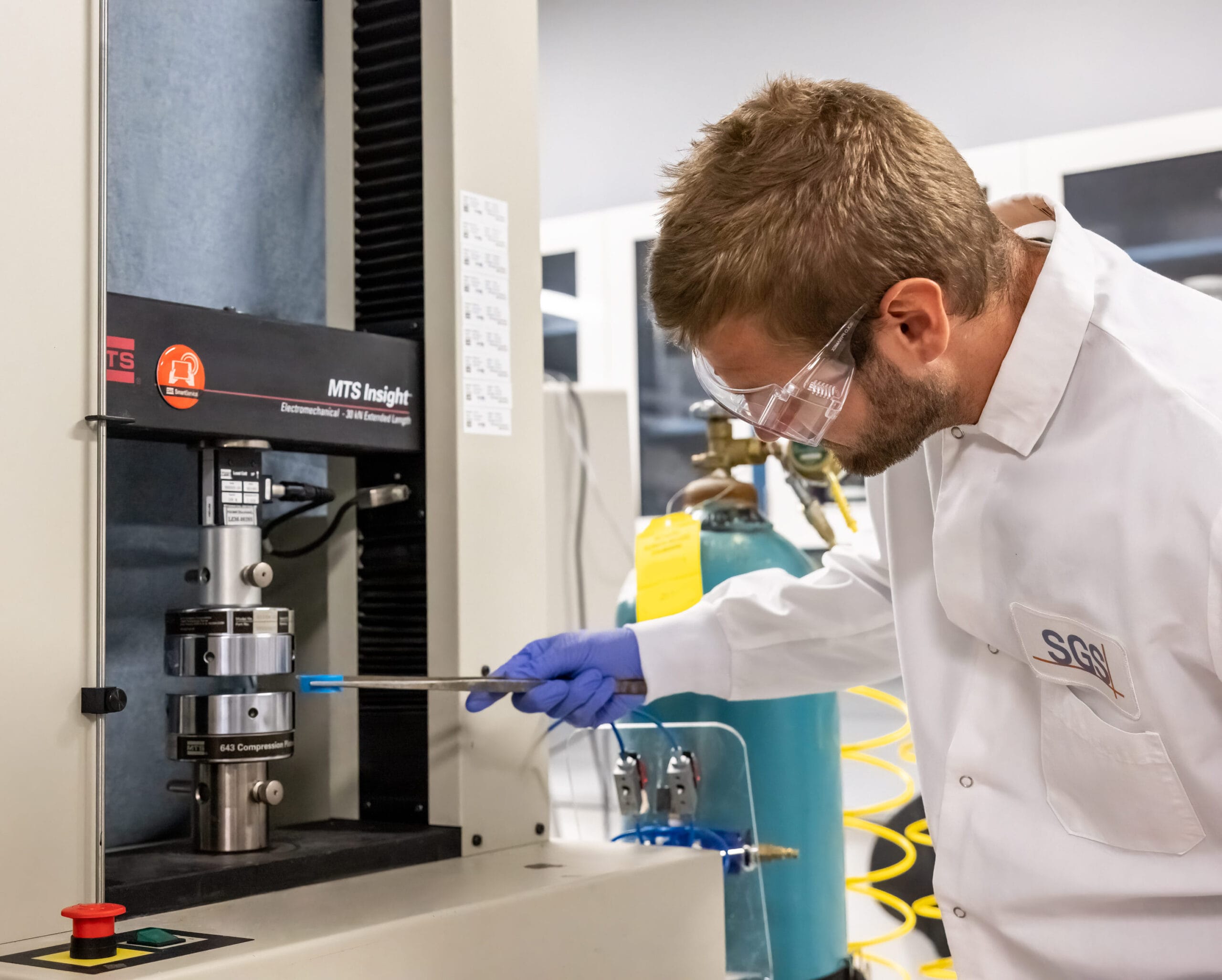
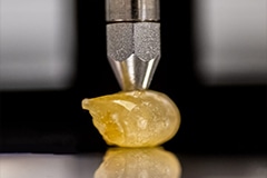
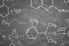
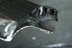
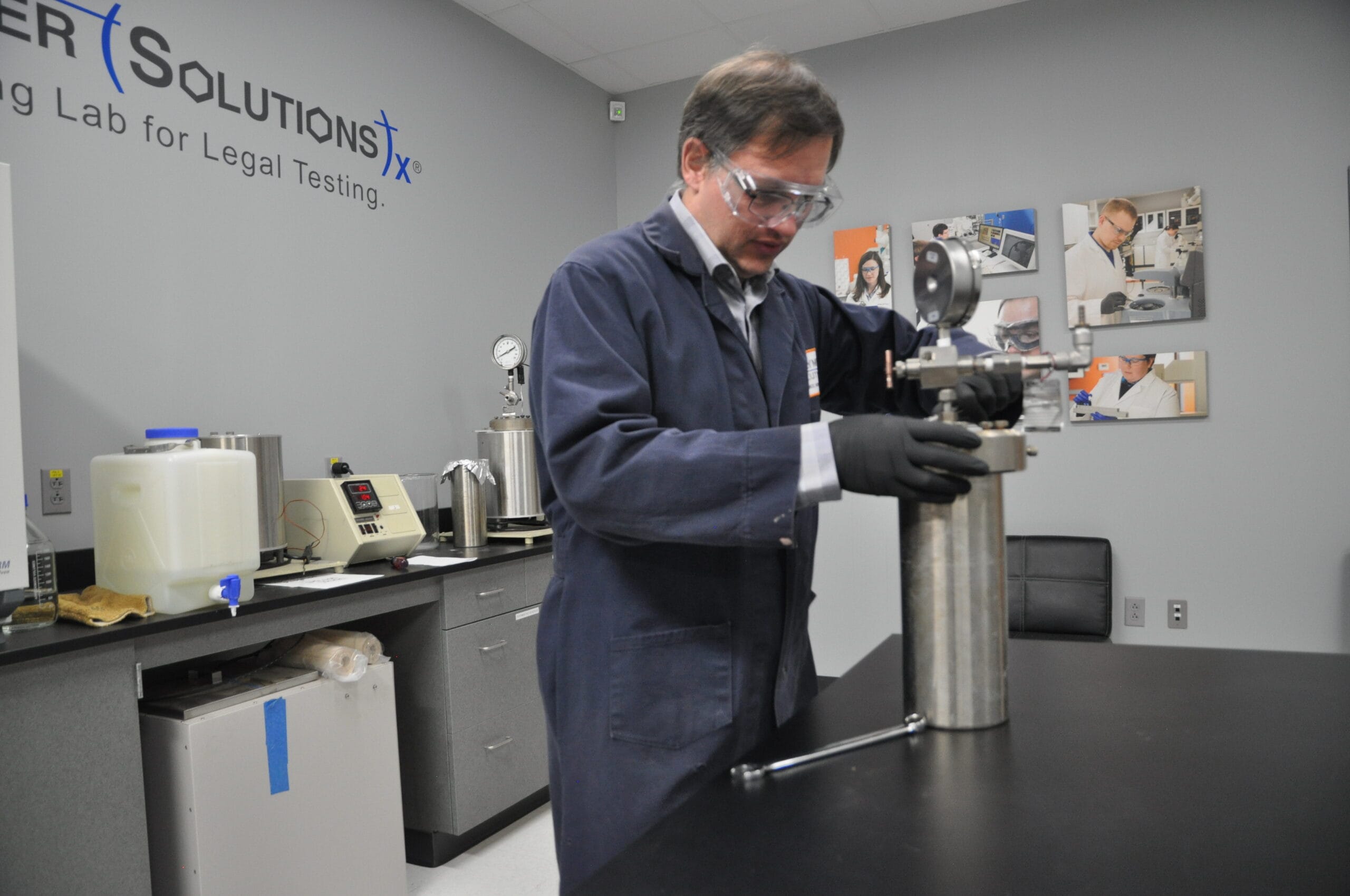
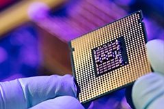
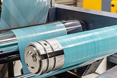
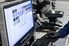
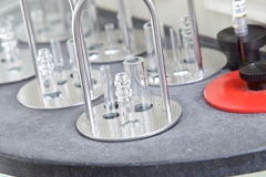
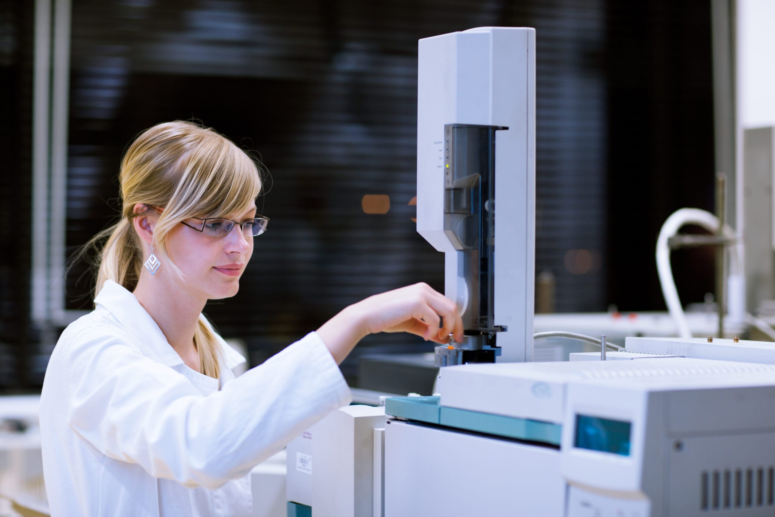
SEM Analysis | SEM-EDS Analysis
Scanning Electron Microscopy (SEM Analysis) can magnify a sample up to 500,000x. Used with EDS it can determine the elements that comprise a sample region.
How does SEM Analysis work?
Scanning Electron Microscopy (SEM) magnifies a specific sample region using a high energy focused beam of electrons. The sample is under vacuum to ensure the electron beam stays focused and does not interact with particles in the air. When the beam of electrons hits the sample, it causes secondary electrons to be released from the sample which are detected to provide an image based off the topography of the surface. The two detectors most commonly used include the Secondary Electron Detector (SED) and the Backscattered Electron (BSE) Detector.The electrons interact with the detector to create an image.
This powerful electron microscope is capable of magnifying up to 500,000 times! SEM Analysis is more powerful than Optical Microscopy not only because of the much increased magnification power but also because of the increase in depth of field.
How does EDS Analysis work?
The sample region evaluated with SEM Analysis can also be analyzed to determine the specific elements that comprise the sample region by utilizing Energy Dispersion Spectroscopy (EDS). X-rays are also released from the surface of the sample that carry a unique energy signature that are specific to elements found in the sample. These X-rays are detected with the EDS detector to give elemental information about the sample. EDS provides data about the chemical composition of the sample and provides additional data about the features that are observed in the SEM micrographs. This combined technique is referred to as SEM-EDS or SEM-EDX Analysis.
Check out the video for our new SEM/EDS
SEM-EDS Analysis is a great method for determining particle sizes and elemental composition. It is also a go-to analytical technique for performing nanocharacterization.
SEM analysis can be performed as part of a film layer analysis to determine the thickness of a film. Not only that, used in conjunction with EDS it is possible to compare different chemical compositions between each layer. The topography of films can at times mask the number of film layers in a sample; elemental mapping can show layers not visible by other methods.
Contamination analysis, identification of filler content, failure analysis, forensic engineering, and fractography are also other common situations in which SEM Analysis pared with EDS is very valuable.
Additionally, the SEM/EDS is a workhorse technique for metals testing such as fractography, embrittlement, corrosion analysis and alloy compositions.
In order to perform this type of analysis the sample needs to be a solid material, it cannot be performed on liquids or gases. Non-conductive samples are sputter coated with gold to prevent electronic charging.
To perform the analysis, the sample must fit into the sample chamber of the instrument, which can accomodate samples that are up to four inches (roughly 10 cm) in the longest dimension and up to approximately one inch (2.5 centimeters) in thickness.
Also, there are limitations on the volatile content of samples because excessive off-gassing can be detrimental to instrument performance.
The above elemental map was captured with SEM-EDS Analysis as part of a contamination analysis project. The image depicts a copper mesh with a silicon contaminant. Red, blue, and yellow indicate the presence of carbon, silicon, and copper (respectively).
Our experience with SEM/EDS Analysis includes:
Products We’ve Tested: