
Spectroscopy
Scanning Electron Microscopy (SEM Analysis) can magnify a sample up to 250,000x. Used with EDS it can determine the elements that comprise a sample region.
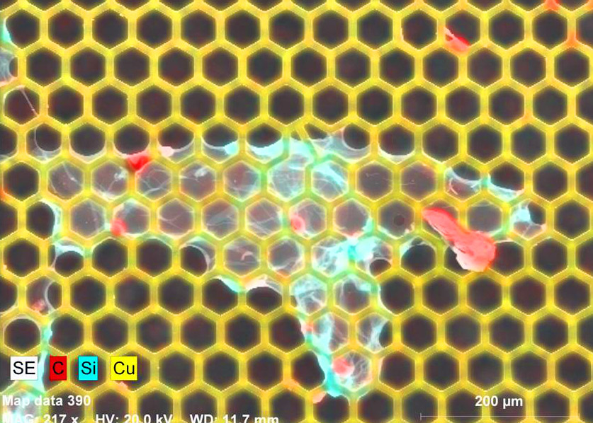
The sample region evaluated with SEM Analysis can also be analyzed to determine the specific elements that comprise the sample region by utilizing Energy Dispersion Spectroscopy (EDS). X-rays are also released from the surface of the sample that carry a unique energy signature that are specific to elements found in the sample. These X-rays are detected with the EDS detector to give elemental information about the sample. EDS provides data about the chemical composition of the sample and provides additional data about the features that are observed in the SEM micrographs. This combined technique is referred to as SEM-EDS or SEM-EDX Analysis.
Check out the video for our SEM/EDS
Approaches
SEM-EDS Analysis is a great method for determining particle sizes and elemental composition. It is also a go-to analytical technique for performing nanocharacterization.
SEM analysis can be performed as part of a film layer analysis to determine the thickness of a film. Not only that, used in conjunction with EDS it is possible to compare different chemical compositions between each layer. The topography of films can at times mask the number of film layers in a sample; elemental mapping can show layers not visible by other methods.
Contamination analysis, identification of filler content, failure analysis, forensic engineering, and fractography are also other common situations in which SEM Analysis pared with EDS is very valuable.
Additionally, the SEM/EDS is a workhorse technique for metals testing such as fractography, embrittlement, corrosion analysis and alloy compositions.
Sample Considerations
In order to perform this type of analysis the sample needs to be a solid material, it cannot be performed on liquids or gases. Non-conductive samples are sputter coated with gold to prevent electronic charging.
To perform the analysis, the sample must fit into the sample chamber of the instrument, which can accommodate samples that are up to four inches (roughly 10 cm) in the longest dimension and up to approximately one inch (2.5 centimeters) in thickness.
Also, there are limitations on the volatile content of samples because excessive off-gassing can be detrimental to instrument performance.
Contact an expert to talk through your specific sample considerations
Experience
Products we’ve tested:
- Metal alloy analysis
- Natural samples, including wood
- Paint and primer layers
- Medical device products
- Filler content from thermoset or thermoplastic materials
- Food packaging
- Grit and powder residue
- Composites
- Ceramics
- Medical Screws
- Medical Implants
- Children’s Toys
- Bullets
- Films
- Woven Materials
Our experience with SEM/EDS Analysis includes:
- Failure analysis of an injection molded plastic part
- Identification of filler content
- Film layer thickness and composition
- Identification of contaminants
- Identification of unknown powders and residues
- Particle size analysis and elemental composition of particles
- Identification of the thickness of coatings
- Weave structure and construction of a specialty medical fabric
- Filler content and composition of plastic compound from a potential alternate supplier