Packaging Material Testing
Microscopy is used for film layer analysis.
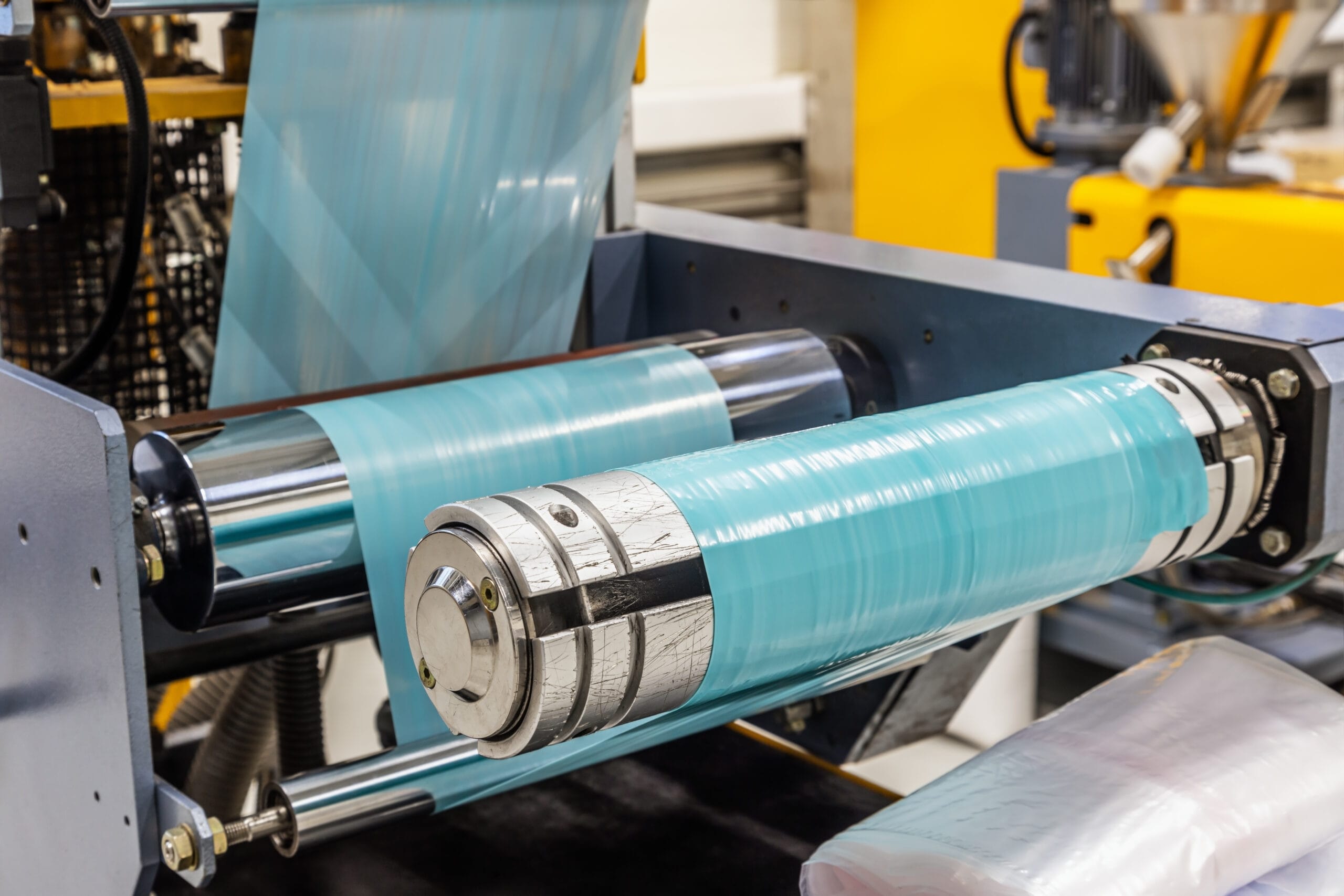
Film technology is extremely complex and is relevant to various industries, including medical device and product, pharmaceutical, food, and consumer product packaging. Films are often composed of several layers where each layer provides a unique property, such as a gas barrier, adhesion, chemical resistance, or oxidation resistance. The combination of layers forms a functional product.
Important reasons for conducting film layer analysis include determination of the thickness and composition of film layers, including both organic and inorganic components. This is done both for manufacturing quality control and for analysis of competitor products.
Approaches
Scanning Electron Microscopy with Energy Dispersive Spectroscopy (SEM-EDS) is commonly used for film layer analysis.
Optical Microscopy is also useful, particularly if layers may be differentiated by color or otherwise optically visualized. The lower magnification range is also useful for thicker samples.
Sample Considerations
The film sample is typically fixated and cross-sectioned.
The required thickness of the film sample is usually below 2 millimeters for SEM analysis. However, thicker films can still be analyzed.
If SEM is the method used for analysis there are limitations on the volatile content of samples because excessive off-gasing can be detrimental to instrument performance.
Please contact us to talk through your specific sample considerations and Film Layer Analysis needs.
Experience
Work we’ve done:
- Layer thickness of films
- Identification and composition of particles in films
- Competitor product analysis and comparative analysis
- Delamination and film adhesion analysis
- Elemental composition of film layers
Products we’ve tested:
- Food Packaging
- Window tinting
- Metalized films
- Film composites
- Product labels
- Plastic bags
- Candy wrappers
- Foil laminated films
- Medical packaging
- Geo-engineering films
- Electronics packaging