Microscopy
SGS Polymer Solutions Incorporated has decades of expertise in microscopy testing and analysis across a range of industries and applications.
We offer optical, electron, and scanning probe microscopy.
Expert, Independent Microscopy Testing & Analysis Services.
Modern microscopy allows us to obtain images from objects that cannot be seen with the unaided eye. The three main branches of microscopy analysis are optical, electron, and scanning probe microscopy.
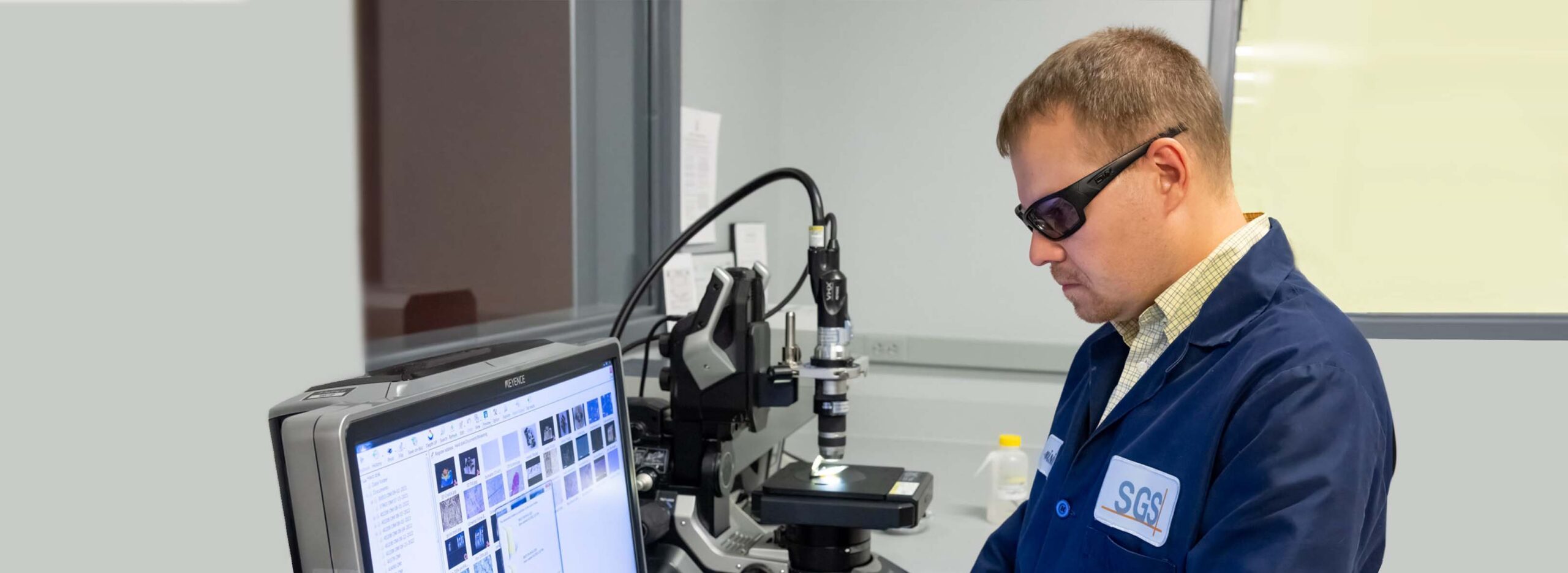
To characterize a sample of unknown morphology, we start with the simplest method of optical microscopy (OM), with a magnification of 10-2,500x, using transmitted light (bright field) for transparent and semitransparent samples or reflected light for opaque samples.
To obtain higher magnification or better resolution, down to micro, nano, and molecular levels, we use Transmission Electron Microscopy (TEM), Scanning Electron Microscopy (SEM) or Atomic Force Microscopy (AFM). We select microscopy methods depending on the application needs and the characteristics of the sample.
Microscopy methods offer a means to understand and characterize the structural features of materials on micro- and nano- scales. The high magnifications provided by transmission and scanning electron and probe microscopies offer value in identifying and assessing subtle variables that can lead to undesirable characteristics, or serve to explain superior performance in a final product. Often, a combination of OM and SEM are the first tools used to assess a surface in a failed part to help determine the cause of the failure, such as whether the part failed in a ductile or brittle fashion.
High-resolution microscopy testing is widely used in material science, polymer composites, particulate analysis, nanotechnology, and semiconductor research. SGS PSI frequently uses microscopy methods to test:
- Nanomaterials
- Textiles
- Films
- Coatings
- Molded Parts
- And many other materials
Microscopy Methods & Approaches
SGS PSI is a microscopy testing lab with 25 years of experience in the following methods:
Optical Microscopy (OM) uses visible light to magnify a sample area 10-2,500x. This microscopy analysis technique often is the first one to be used before additional microscopy testing.
Transmission Electron Microscopy (TEM) uses an electron beam passing through a very thin slice of the specimen, and contrast is generated from differences in electron densities. Staining may be used to increase contrast. The method is useful for examining polymers and biological structures with nanometer resolution.
Scanning Electron Microscopy (SEM) scans the surface of the sample with a highly focused electron beam to obtain a surface image. SEM can be coupled with Energy Dispersive Spectroscopy (EDS) for determination of the elemental composition of the sample.
Atomic Force Microscopy (AFM) uses a mechanical cantilever with a sharp tip to scan a flat specimen surface with highest resolution down to a fraction of a nanometer. It can work in ambient conditions.
Optical Birefringence is used to assess existing mechanical stress in transparent materials. The sample is examined in a nondestructive way between cross-polarizing filters.
Image Analysis allows our scientists to extract meaningful information, such as size and geometry of morphological characteristics, from the microscopic images.
Microscopy Applications & Experience
Common applications of microscopy testing and analysis include:
- Analyzing the uniformity, size, and distribution of filler components in a composite sample
- Measuring the layer thickness of multilayer products
- Determining the phase morphology of a material
- Contamination analysis
- Competitor product comparison and analysis
- Product failure analysis investigation
- Fractography analysis
- Analyzing the uniformity, thickness, and porosity of a coating
SGS Polymer Solutions Incorporated has ISO/IEC 17025 accreditation and FDA registration. Our scientists have decades of experience using microscopy testing and analysis for:
- Part dimensions
- Particle size distribution
- Fiber dimensions
- Failure analysis
- Morphology
- Pigment dispersion