Microscopy
Optical profilometry provides comprehensive surface analysis that’s precise, efficient and contact free to protect your delicate samples.
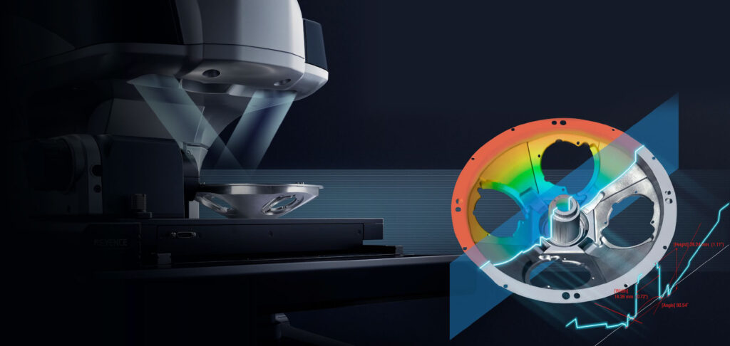
We’re redefining surface measurement with advanced, non-contact 3D surface analysis. Using the Keyence VR-6200 Optical Profilometer, our scientists capture surface roughness, texture, and defects with precision – no contact, no damage, just flawless results.
From jet engine components to medical devices, optical profilometry is ideal for identifying fine texture variations, evaluating coatings and performing failure analysis or quality control. Cross section measurements can be performed with no blind spots and wall thicknesses and recessed features can be measured without cutting or destroying your sample.
- 3D Surface Profiling: Captures detailed 3D images of surface topography with micron or sub-micron accuracy.
- Non-contact Measurement: Uses optical technology (typically white light interferometry or confocal microscopy) to avoid damaging delicate surfaces.
- High-Resolution Scanning Data: Delivers precise measurements of roughness, waviness, step heights, and flatness.
- Testing Versatility: Suitable for polymers, composites, metals and more. We analyze your products surface defects, coatings, wear, or microstructures.
Measurement Capabilities
- Profile measurement: height differences, chamfers, draft angles, radii.
- 2D measurement: distances and angles between circles, points, and lines.
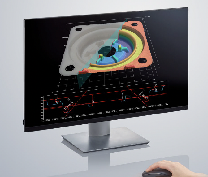
- 3D measurement: perform non-destructive cross-sectional analysis. CAD comparison and CAD conversion
- Surface Roughness
- GD&T measurement (Geometric Dimensioning and Tolerancing)
Scanning area:
167mm X 300mm X 150mm H x L x W (6.57” x 11.81” x 5.91” H x L x W)
Stage Load capacity:
4.5 kg (9.92lbs)
Rotational Unit Capacity:
1kg (2.2lbs)
Magnification Range:
Low magnifications: 12x, 25x, 38x, 50x
High magnifications: 40x, 80x, 120x, 160x
Height Measurement:
Repeatability: Without Z stitching: 0.4 µm With Z stitching: 1.0 µm
Measurement accuracy: Without Z stitching: ±2.5 µm With Z stitching: ±4.0 µm
Width Measurement:
Repeatability: Low Magnification: 1µm High Magnification: 0.5 µm
Measurement accuracy: Low Magnification: ±5µm High Magnification: ±2 µm
Surface Analysis:
Resolution: 0.1 µm
Roughness: 42 total roughness parameters can be measured, Ra,Rz,Sa and Sz. ISO 4287 (1994, 2001) and ISO 25178 compliant.
Applications
- Performing failure analysis or quality control for precision components
- Dimensional analysis of micro-components in electronics, like PCB solder joints
- Evaluating surface finish and texture after machining or polishing
- Surface roughness measurement for materials like metals and plastics
- Surface texture analysis for quality control in additive manufacturing
- Burr and defect inspection on machined parts
- 3D shape and profile analysis, such as tire tread patterns
- Flatness and step height measurement after processes like etching
- Film thickness and sub-surface measurements using techniques like white-light interferometry
- Wear and erosion assessment on mechanical parts, such as gears or bearings
- Measurement of coating thickness uniformity in industries like aerospace
- Analysis of micro-fluidic channel profiles in medical device manufacturing
Sample Considerations
Sample preparation is typically minimal, which is one of its key advantages of this instrumentation. The ideal sample size depends on what you’re measuring, and we recommend you contact an expert to discuss your specific testing needs and associated sample considerations.